About Us
 Belford Research Inc. is a Microelectronics Research Company specializing in Electronic/optical Materials, in particular changing the properties of existing advanced microelectronic materials. Single Event Radiation Hard Microelectronics can be achieved by applying our processes to post-processed wafers. Our main function is to improve the capability of existing semiconductors and manufactured ICs by changing their physical state and bonding to final substrates. New Manufacturing Processes produce ultra-fast, rad-hard CMOS devices. This work impinges on high-speed electronics for robust applications.
Facilities
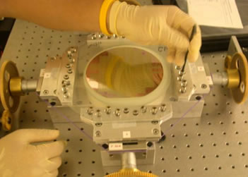
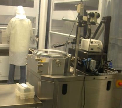
The company premises were custom built to house 3300 sq. ft. of laboratory space. Laboratory facilities include a class-100 clean room, with dedicated air handlers and extraction facility. Several class 100 clean stations are equipped with laminar flow and extraction. Our working environment exceeds this standard and approaches class 10 conditions. The clean room function is in the main direct wafer bonding and plasma activated wafer bonding.
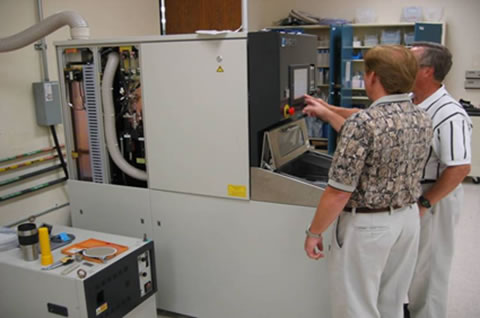
Wafer thinning facilities include a DAG810 Grinder (Disco) and for sub 80 micron wafer thickness a MemsStar XeF2 Dry Etcher & Remote Plasma System. Our three separate Mechanical straining facilities are housed independent softwall clean rooms. Facilities include semiconductor grade chemical processing: silicon wet and dry etching, front side IC protection, spin coating, direct, and indirect wafer bonding and polymerization techniques.
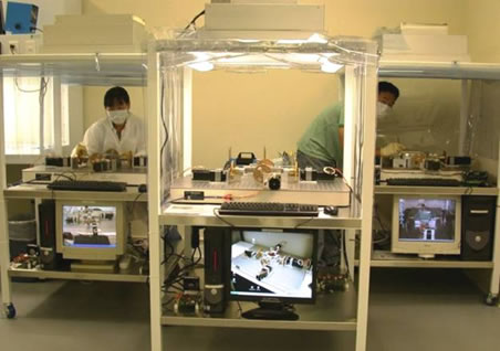
Our engineering lab houses 2 laminar work Bridgeport milling machine and bench-top lathe. The optics lab includes semiconductor surface and sample thickness determination equipment, and computer controlled high power 4 lens (x1000) microscope with Nomarski prisms and video capture.
The electronics (test) lab is equipped with an 8" probe station and an Agilent 4155C semiconductor parameter analyser.